
https://wemarketresearch.c...

View Full Report: https://dataintelo.com/rep...
The global CMP (Chemical Mechanical Planarization) Equipment Market is poised for significant expansion, driven by the growing adoption of advanced semiconductor manufacturing technologies. With the increasing demand for miniaturized and high-performance electronic devices, CMP equipment has become a critical component in the semiconductor industry. According to DataIntelo, the market is projected to witness substantial growth in the coming years, fueled by technological advancements and rising investments in the semiconductor sector.

CMP Equipment Market Share, Trends & Analysis | 2032
The CMP equipment market was valued USD 2.3 Billion in 2023 and is expected to reach around USD 3.6 Billion by 2032 with a CAGR of 5.3% during the forecast period 2024-2032.
https://dataintelo.com/report/cmp-equipment-markethttps://dataintelo.com/rep...
The Heating Jacket for Semiconductor Market is rapidly gaining momentum as the semiconductor industry intensifies its focus on thermal management and process efficiency. Heating jackets are critical in ensuring optimal temperature control during the processing of advanced semiconductor materials, reducing contamination risks, and maintaining high yield production.
As chip designs become more complex and sensitive to thermal variation, heating jackets offer a stable and uniform heat environment—making them indispensable in next-generation fabrication technologies.

Heating Jacket for Semiconductor Market Report | Global Forecast From 2025 To 2033
The global heating jacket for semiconductor market size was valued at approximately USD 800 million in 2023 and is projected to reach around USD 1.5 billion by 2032, growing at a compound annual growth rate (CAGR) of 7%.
https://dataintelo.com/report/global-heating-jacket-for-semiconductor-marketGet an EXTRA 20% OFF your hosting plan!
Hostinger's got a HOT deal! Get an EXTRA 20% OFF your hosting! Don't miss out!


Takshila-vlsi.com test training design will enable you to realize your full potential. Acquire valuable skills and advance your career in the semiconductor industry.
https://www.takshila-vlsi....

Read More -> https://dataintelo.com/rep...
The global Through Glass Via (TGV) Technology Market is poised for remarkable growth, driven by advancements in semiconductor packaging, consumer electronics, and the rising demand for miniaturized electronic components. According to a recent report by Dataintelo, the market is projected to grow at a CAGR of 18.5% from 2023 to 2030, reaching a valuation of USD 1.2 billion by the end of the forecast period.
TGV technology, a cutting-edge innovation in the semiconductor industry, enables the creation of high-density interconnects through glass substrates. This technology is gaining traction due to its superior electrical performance, thermal stability, and ability to support advanced packaging solutions. The increasing adoption of TGV in applications such as 5G devices, IoT, and automotive electronics is fueling market expansion.

Through Glass Via (TGV) Technology Market Research Report 2032
The global Through Glass Via (TGV) technology market is on an impressive growth trajectory, with a market size estimated at USD 450 million in 2023, projected to reach USD 1.3 billion by 2032, registering a robust compound annual growth rate (CAGR) of 12.5%.
https://dataintelo.com/report/through-glass-via-global-technology-marketThe Global Semiconductor Filter Market size is expected to be worth around USD 3,062.7 Million By 2034, from USD 1,293.7 Million in 2024, growing at a CAGR of 9.00% during the forecast period from 2025 to 2034. Asia-Pacific dominated the semiconductor filter industry in 2024, accounting for over 49% of the market share and generating USD 633 Million in revenue.
Read more - https://market.us/report/s...
The Semiconductor Filter Market refers to the industry focused on producing and supplying specialized filtration systems used in semiconductor manufacturing. These filters are critical for maintaining ultra-clean environments by removing contaminants like particles, gases, and chemicals from air, liquids, and gases used in processes such as photolithography, etching, and chemical mechanical planarization. The market caters to the semiconductor industry’s need for high-purity conditions to ensure the quality and reliability of chips, which are integral to electronics, automotive, telecommunications, and healthcare sectors. As chips become smaller and more complex, the demand for advanced filtration solutions grows, driven by the need for precision and defect-free production. This market includes various filter types, such as air, liquid, and gas filters, each designed to meet stringent industry standards.
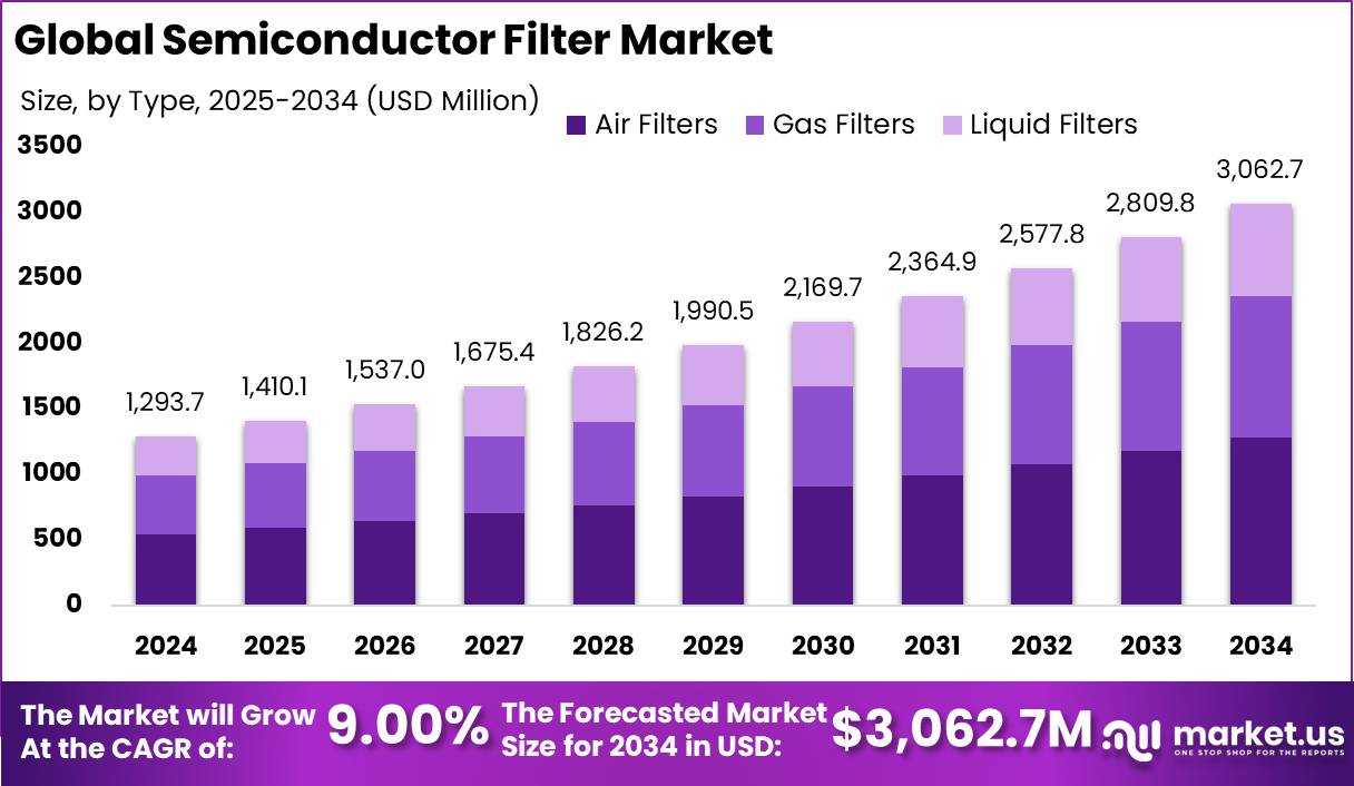
Semiconductor Filter Market Size | CAGR of 9%
Semiconductor Filter Market is estimated to reach USD 3,062.7 Million By 2034, Riding on a Strong 9% CAGR throughout the forecast period.
https://market.us/report/semiconductor-filter-market/Understanding the Fundamentals of Epitaxial Wafers and Their Applications
Epitaxial wafers have become a crucial component in the semiconductor industry, playing a vital role in the fabrication of advanced electronic devices. These wafers are created through a process called epitaxy, which involves growing a single-crystal layer on top of a substrate wafer. The resulting epitaxial layer possesses the same crystallographic orientation as the substrate, ensuring high-quality and uniform material properties.
Epitaxial Wafer find extensive applications across various sectors, including consumer electronics, automotive, healthcare, and telecommunications. They are used in the production of light-emitting diodes (LEDs), power devices, radio frequency (RF) devices, and microelectromechanical systems (MEMS). The unique properties of epitaxial wafers, such as precise control over dopant concentration and layer thickness, enable the fabrication of high-performance and energy-efficient devices.
Epitaxial Wafer -https://www.coherentmarket...

https://dataintelo.com/rep...
The AMHS for Semiconductor Market is witnessing exponential growth as semiconductor manufacturers ramp up automation to meet escalating global chip demand. Automated Material Handling Systems (AMHS) are becoming vital to modern fabs, optimizing production throughput, reducing contamination risks, and improving operational efficiency. As the semiconductor industry faces mounting pressure for precision and scalability, AMHS adoption is emerging as a strategic imperative.

AMHS for Semiconductor Market Report | Global Forecast From 2025 To 2033
The Automated Material Handling Systems (AMHS) for the semiconductor market size is projected to grow from USD 2.5 billion in 2023 to an estimated USD 5.6 billion by 2032, at a compound annual growth rate (CAGR) of 9.5%.
https://dataintelo.com/report/global-amhs-for-semiconductor-marketElectrostatic chucks, also known as electrostatic clamps, are widely used in fabrication steps within the semiconductor industry. They are used for holding and positioning silicon wafers securely during various microelectronic manufacturing processes such as plasma etching and physical vapor deposition.
Electrostatic Chucks Market - https://cmi.hashnode.dev/e...
#ElectrostaticChucks #SemiconductorManufacturing #WaferProcessing #ElectrostaticChucksMarketShare #CoherentMarketInsights
https://dataintelo.com/rep...
The Semiconductor Grade High-Purity Ammonia Market is witnessing a significant surge as the global semiconductor industry continues to expand. This ultra-refined chemical compound, critical in the manufacturing of integrated circuits and other microelectronics, is essential for ensuring contamination-free deposition processes in semiconductor fabrication.
As of 2024, the global market for semiconductor grade high-purity ammonia is valued at USD 397.5 million, and is projected to reach USD 691.8 million by 2032, growing at a CAGR of 7.1% during the forecast period. The rising demand for advanced consumer electronics, 5G infrastructure, and electric vehicles (EVs) is directly driving growth in this specialized chemical segment.

Semiconductor Grade High-Purity Ammonia Market Report | Global Forecast From 2025 To 2033
In 2023, the global semiconductor grade high-purity ammonia market size was valued at approximately USD 1.2 billion.
https://dataintelo.com/report/global-semiconductor-grade-high-purity-ammonia-marketView Full Report: https://dataintelo.com/rep...
The global semiconductor valve market is experiencing significant growth, driven by the rising demand for semiconductor manufacturing equipment, technological advancements, and increasing applications in consumer electronics, automotive, and industrial sectors. As the semiconductor industry continues to expand, the need for high-performance valves to regulate gas and liquid flow in production processes is expected to surge.
View Full Report: https://dataintelo.com/rep...
The global Semiconductor FFKM O-ring Market is experiencing robust growth, fueled by increasing applications in the semiconductor industry. As technological advancements continue to drive the need for high-performance sealing solutions, the demand for FFKM O-rings is surging across key regions. The market is expected to witness substantial expansion in the coming years, driven by factors such as growing semiconductor manufacturing, rising investments in chip fabrication, and stringent industry standards.

Semiconductor FFKM O-ring Market Research Report 2032
The global semiconductor FFKM O-ring market size was valued at approximately $X billion in 2023 and is expected to reach around $Y billion by 2032, growing at a CAGR of Z% during the forecast period.
https://dataintelo.com/report/global-semiconductor-ffkm-o-ring-marketThe discrete semiconductor industry is accelerating under the weight of electrification, renewable energy systems, and sophisticated power management across sectors. Expert buyers and OEMs are leveraging advanced process nodes to unlock market opportunities in automotive, industrial, and consumer electronics applications.
Get more insights on Discrete Semiconductor Market – https://articlescad.com/di...
#DiscreteSemiconductorMarket
#DiscreteSemiconductorMarketGrowth
#DiscreteSemiconductorMarketDemand
#DiscreteSemiconductorMarketTrend
#CoherentMarketInsights
https://www.maximizemarket...
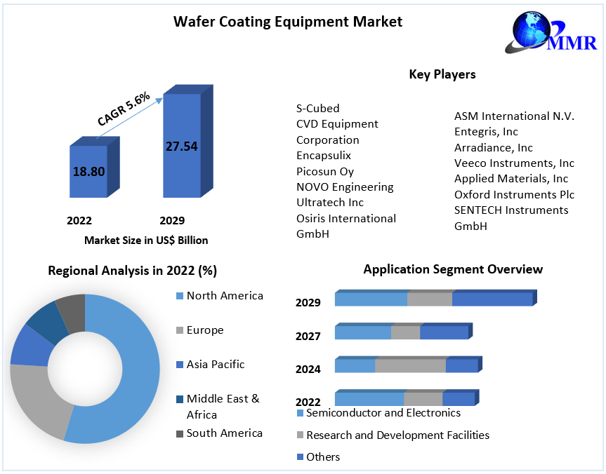
Wafer Coating Equipment Market – Global Industry Analysis and Forecast
Wafer Coating Equipment Market is expected to reach US$ 27.54 Bn. by 2029, at a CAGR of 5.6% during the forecast period.
https://www.maximizemarketresearch.com/market-report/global-wafer-coating-equipment-market/76792/